Invited Talk
"Empowering the AI Era: Emerging Memory Solutions for the AI Era"

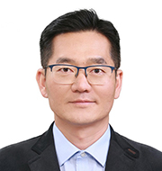
Dr. Taeksang Song
Corporate VP at Samsung Electronics
Abstract
The rapid growth in data generation and complex workload requirements has led to increased computational power, enabling the development of sophisticated, large-scale AI models. This shift necessitates advanced GPUs and enhanced memory solutions for learning and inference. These solutions must provide substantial bandwidth, capacity and power-efficiency to support proliferated multimodal AI models. In this talk, we will explore cutting-edge memory products and technologies essential for various AI applications, highlighting how CXL memory modules can be tailored to optimize performance across each application. Some of the main technologies we will cover include cutting-edge DRAM technologies such as MRDIMM and LPCAMM.
Bio
Taeksang is a Corporate VP at Samsung Electronics where he is leading a team dedicated to pioneering cutting-edge technologies including CAMM, MRDIMM, CXL memory expander, fabric attached memory solution and processing near memory to meet the evolving demands of next-generation data-centric AI architecture. He has 20 years' professional experience in memory and sub-system architecture, interconnect protocols, system-on-chip design and collaborating with CSPs to enable heterogeneous computing infrastructure. Prior to joining Samsung Electronics, he worked at Rambus Inc., Micron Technology and SK hynix in lead architect roles for the emerging memory controllers and systems.
Taeksang receives his Ph.D. degree from KAIST, South Korea, in 2006. Dr. Song has authored and co-authored over 20 technical papers and holds over 50 U.S. patents.
"Device technologies of NAND flash with emphasis on fundamental physics"

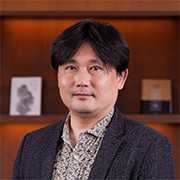
Dr. Seung Jae Baik
Samsung Electronics
Abstract
In this talk, historical evolution of three dimensional NAND flash technology is reviewed and a list of published device technologies are explained. In addition, fundamental topics about charge storage phenomena and a design for secure charge storage are covered.
Bio
Seung Jae Baik received the B.S., M.S., and Ph.D. degrees in electrical engineering from the Korea Advanced Institute of Science and Technology (KAIST), Daejeon, South Korea, in 1994, 1996, and 2001, respectively. From 2001 to 2009, he was with Samsung Electronics Company Ltd., Yongin, South Korea, where he contributed to novel Si devices, high-density flash memory devices, and charge trap flash memory devices, as a Senior Engineer and a Principal Engineer. From 2009 to 2012, he was with KAIST as a Research Professor, where he contributed to thin film Si solar cells, quantum dot solar cells, new memory materials, and devices. From 2012 to 2022, he was with Hankyong National University, Anseong-si, South Korea, as a Professor. Since 2023, he again has been with Samsung Electronics, Co, South Korea. His current research interests are focused on high density NAND flash memory and progressive concepts in memory field. He has authored and co-authored over 50 technical papers.
"Design Technologies for Vertical NAND Flash Memory"

Dr. Cheon An Lee
Samsung Electronics
Abstract
In this talk, various kinds of technologies for current and future VNAND Flash Memory will be introduced, with a focus on the design point of view. Reduction of VNAND chip size, enhancement of core performance, and high-speed I/O are key driving forces for the development of VNAND design technologies, and there have been numerous technology developments to meet product needs. Key design technologies for each category will be discussed in this presentation.
Bio
Cheon An Lee received the B.S. and M.S., and Ph.D. degrees in electrical engineering from Seoul National University, Seoul, Korea, in 2000, 2002, and 2007, respectively.
In 2007, he joined the DRAM Design Team of Samsung Electronics Corporation in Gyeonggi-do, Korea, and was involved in developing 40nm DRAM Design. In 2009, he moved to the Flash Design Team and worked on cell physics, analog and core circuit design, and peripheral transistors for vertical NAND Flash memory. Since 2022, he has been working on circuits and devices for the next-generation VNAND at the Advanced Flash Technology Team. He is currently a Master with Samsung Electronics Company Ltd. His current research interests include circuit design, peripheral transistors and cell devices for Flash memory.

